widgets

Monday, 26 May 2014

Project recommendation.

The followings are the recommendation in order to enhance the project quality and performances:
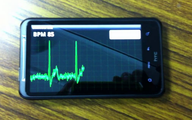
ECG android system


  1. The circuit should have more amplification and filtering to maximize its output quality and tracking system.
  2. This project should connect into the android system hence the user can see their own ECG continuously in smart phone application (in real time). Hence, the result obtain can be share in the world wide which has internet connectivity.
  3. The electrode sensor which is a cooper plate should attach together with the Velcro strip to minimize the setting procedure.
  4. The electrode is exchangeable so that user can use the conventional disposable ECG electrode which is cheap and easy to use.
  5. The circuit design can be improved from 2 electrode sensors to 6 electrode sensors. In other word, instead of using bipolar leads, this project should be very precise and efficient by using precordial leads.
  6. The improvement of software part should be made by adjusting the software block diagram in LabVIEW. To do this, a research have to be done to study and exploring this software because the block diagram in this software must include filter block to minimize noise. 
Although the project output was not in the same level of quality to be compared with conventional ECG machine used by most of hospitals in Malaysia but the knowledge and principle of this project is very useful for a medical electronics student and a fresh medical engineer. 

Project Conclusion

This project is significant with medical electronics studies because nowadays medical equipment plays an important role in the treatment and in the medical education. It was constructed in order to enable the students and end-users to comprehend how the ECG works. The ECG with a less complex circuit performing the basic function will enable them to understand how the signal is obtained.The main challenges include amplifying the desired This project are successfully run and achieve its target in a low budget as stated earlier. It is very important to do a beneficial project with minimizing its costing because the main target user of this project is a student and anyone in education field.


Since this project is successfully display the waveform of the electrical activity of heart through a computer which is safe, measureable, affordable, reliable and timely (SMART). Hence, all the objectives have been achieved through this project. The work finding will be very useful to encourage the medical electronics engineering skills further to be a reference for other student to develop a better project and advanced.

Result comparison between project's output and conventional ECG machine

We can compare the result of this project's output and conventional ECG machine. The comparison is divided into 2 parts which is its baseline and linearity.

BASELINE

Baseline position is the position of the wave at the x-axis and y-axis ( 0,0 ). The graph can only have ±5 mm error from the baseline and this baseline based on the first graph (at the left side). When measured the baseline position at the graph paper it should consist only ±5 mm.

Result obtain from this project


Result from conventional ECG machine

Both of graph show an acceptable value of error which is below ±5 mm. However this project contain much higher baseline error value of ±2.45 mm to be compared with baseline error value of  ±0.2 mm for the conventional ECG machine. Hence, the baseline condition for the conventional ECG is much more accurate, stable and acceptable. This problem should be utilise to increase to have a precise baseline by setting an accurate and correct range of amplitude of Y axis and time for X-axis. It can be done with the use of properties button in the LabVIEW software.

LINEARITY

For linearity based on the print out graph either it in linear or not and the result is still acceptable if the is only have ±5 % error. Picture below show the linearity of the ECG machine which measured by a straight blue line as an indicator. 

Result obtain of this project

Result from conventional ECG machine

Both of the waveform shown a different percentage of linearity which is the conventional ECG linearity is much more stable and accurate to be compared with the project linearity. As a solution to this problem, a lower gain should be applied to this project to ensure its stability and accuracy. 

High and low gain of ECG machine

Since the project has high and low gains switch hence there a quality difference between the two gains. In this project, gain is a measure of the ability of the amplifier is to increase amplitude of a signal from the input to the output. It is a mean ratio of the signal output of a system to the signal input of the same system.

HIGH GAIN


LOW GAIN


When the switch was in a higher gain, the higher amplification factor applied, and thus any noise will be amplified more. As shown in figure 4.1, the waveform is not stable and weak in linearity. The higher gains maximize its amplitude and ease the user to see the R and R interval for measuring purpose. However, in order to get a stable and accurate output, the user should lower the gain. 

ECG project result

Subject are being asked to lay on a bed to measure her resting heart rate from the wrists. The output displayed on computer screen via LabVIEW.

Project connection between PC, DAQ cad and hardware box of circuit

The waveform displayed are similar with the typical ECG waveform which consist of P, QRS complex and T wave. Normal resting heart rate  is between 60 (beats per minute) and 100 (beats per minute).


The out put waveform which appear in PC

The result of 84 bpm is within this range indicate that this subject is healthy and her heart are pumping normally.  The calculation for heart beat measurement is as below:


Hence, the output of this project are acceptable and its complete the objective which to appear the output on PC screen.

Change from the Visual basic to LabVIEW software

Salam..hi..I have changed the project's software from Visual Basic to LabVIEW. Since DAQ card is used in this project which acts as the interface between a computer and bio-potential signals from both wrist. Hence, LabVIEW software are applied to complete the interfacing part. DAQ card is connected to a computer through a slot or port. 

The DAQ card of NI USB 6210

LabVIEW programs are called virtual instruments or VIs, because their appearance and operation often imitate physical instruments, such as oscilloscopes and multimeters. LabVIEW contains a comprehensive set of tools for acquiring, analyzing, displaying, and storing data, as well as troubleshoot code. Hence this project block diagram are also been changed.

Project's block diagram
The Analogue to Digital Converter functions in DAQ card is to convert a continuous quantity to a discrete time digital representation so that the output could be read by the computer. An ADC may also provide an isolated measurement. This will ensure the data from the ECG could be displayed easily in the computer.

The newest version of LabVIEW
Hence, this project will have a better output waveform which appear on PC screen because in LabVIEW software it self have the filtering function to minimize noise.

Wednesday, 14 May 2014

Etching the PCB board.

Etching is the process to cut the unprotected part in our PCB board. In the previous post, I have mention the use of permanent marker to highlight the printed part of the PCB board. The ink from this permanent marker will protect the circuit area. For those who have no experience doing this activity, now its the right time to learn. First we need to have the ferric chloride, hot water and a bucket. 

Ferric chloride powder

Why we need hot water? Etching at ambient temperature might take over an hour, so its better to heat up the etching solvent to about 35-45 degrees Celcius. Then we need a bucket to dissolved it (ferric chloride) in a clear liquid (hot water) and put the PCB board in it. 


Dissolved the ferric chloride with hot water

The etching takes about 15-30 minutes to be done. But remember at higher temperatures the etching performance decreases. The etching process is an exothermic reaction, it generates heat. Take care, cool your etching tray when necessary! You should minimize the amount of copper to etch by creating copper area in your PCB layout as much as possible. When starting the etching process and little to etch it is difficult to keep the etching solution at 35-45 degrees Celcius.

Shake the bucket

At the end of this procedure we have to make sure all the unprotected part have been removed from the PCB board. After etching, we have to drill the PCB board according to its PCB layout and then we can put all the components through the PCB board. 

Soldering the components on PCB board


Finally we need to solder all the components in the PCB board. Soldering is a process in which two metal items are joined together by melting procedure. Thoroughly coat the soldering tip in solder. It is very important to cover the entire tip. You will use a considerable amount of solder during this process and it will drip, so be ready. If you leave any part of the tip uncovered it will tend to collect flux residue and will not conduct heat very well, so run the solder up and down the tip and completely around it to totally cover it in molten solder. After you are certain that the tip is totally coated in solder, wipe the tip off on the wet sponge to remove all the flux residue. Do this immediately so there is no time for the flux to dry out and solidify.


Saturday, 26 April 2014

Process of constructing the hardware

Firstly, when the circuit has been tested, it was designed using Diptrace PCB Layout. You can also design the layout using Eagle software or Proteus 7 professional. PCB Layout is a software to draw and design the circuit. The advantage of using a PCB is it eliminates or reduces the need of jumper wires as when we utilise a strip board. The longer jumper wire contributes to a noisy signal.


The PCB layout 
After the circuit has been designed, it was then printed on an overhead projected (OHP) paper.  Make sure that we use laser printed ink as a toner transfer ink. Otherwise, you will never get to transfer the ink from OHP paper to your PCB board.


Materials for etching process

                               Make sure you rub the PCB board with sandpaper before you start.


Equipment for etching process and a driller for PCB board


The 
circuit on the blank PCB was made by a toner transfer method where the printed paper was pressed to it by applying high temperature. I spent around 15 minutes to ensure the toner fully transfer to the PCB when a hot clothes iron was applied to the OHP paper. 


The PCB then picked up the ink from the paper, making a print. The ink must stick to the printed circuit board before the board is being etched so that the copper would not scrape off during etching. To ensure the ink or the line is clearly printed on the PCB board, we can use a black permanent maker to highlight the ink.


Finally, we can start ecthing the PCB board!!! 

Friday, 18 April 2014

Tips to buy the components..Lets get start!

I'm really excited to buy all of my FYP components but I'm fuzzy on choosing the best place for electronics components. Hence, I have done my research to choose the place to go for shopping and yes....The best is at JALAN PASAR. Where?? It is located in Pudu, Kuala Lumpur.


You need to list up all the components which you want to buy including its value and type. Then you just pass it to the sales assistance and they will take it for you. It is highly recommended for you to follow them and check each of the components that you already list up. There are so many electronic shops there, so that you don't have to worry if you not found some of the components in one shop. Just walk out from that shop and search in other shop (maybe you have to survey the prices first before you buy).


One thing for sure, it really hard to find my medical instrumentation amplifier which is AD623AN. I went to Jalan pasar and search all over the area and finally I found it in my fourth visit at CALTRUS SDN BHD. The shop seems like too small to have everything, but you can anything in that shop. If they don't have it, they will order the component just for you.


Alhamdulillah..im done for my components part. Before we leave Jalan Pasar, we just have to ensure that we have all the components listed or otherwise you will visit Jalan Pasar again.

Monday, 17 February 2014

Owh no...my USBMOD3 doesn't seem to be working.


To save cost I decided to buy a cheaper USBMOD3 in the internet through MUDAH.my. Yes, it is not new but it is still fully function although there are 2 pins which is considered broke. I just need to solder a new pin in the empty pin hole before I use it. Then I start to run test to make sure it is really worth it to buy a second hand device. Hehe =)

At home, after thousand times connect this USBMOD3 device to my PC, it still doesn't appear anything on screen such as "found new hardware" . Owh no! My USBMOD3 doesn't seem to be working. I want my money back!! =(

When I look at the internet, read all the review about this device, then I realise that in order to make the USBMOD3 to detect under any operating system we will need to connect some module pins to each other as mentioned in the datasheet. Otherwise the module will appear dead, this is because of the different powering options which can be used. Owh yes! =D

The pins which we need to connect to each other on the module are as follows. 

1) Connect EP (pin 9) to RSTO (pin 10)
2) Connect VIO (pin 12) to V+ (pin 13)
3) Set PCTL to low (connect to the device ground)


The schematic view


My USBMOD3 connection
At the end, I just want to say Alhamdulillah because my USBMOD3 is finally working!! (Save almost RM300) =D